- 您现在的位置:买卖IC网 > Sheet目录473 > MAX2634EVKIT+ (Maxim Integrated)KIT EVAL FOR MAX2634 AUTO AMP
�� �
�
�MAX2634�
�315MHz/433MHz� Low-Noise�
�Amplifier� for� Automotive� RKE�
�RF� Input� Coupling� Capacitor�
�Input� IP3� vs.� Enable� Time�
�The� value� of� the� coupling� capacitor� affects� input� IP3�
�and� turn-on� time.� A� larger� coupling� capacitor� results� in�
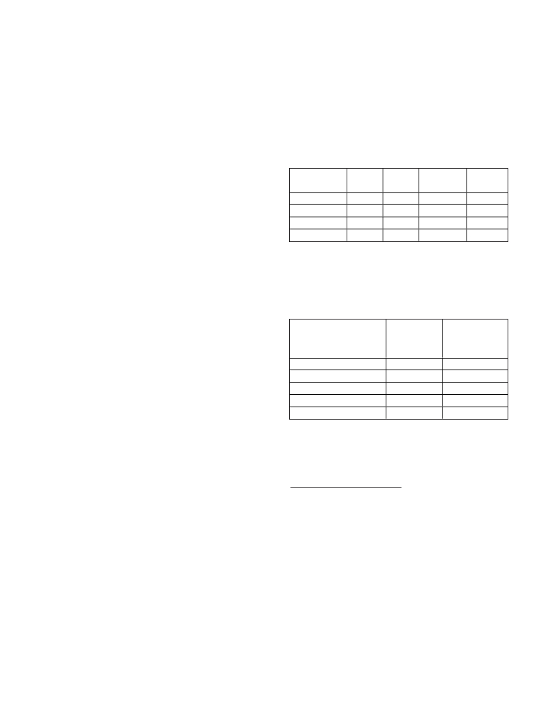
�Table� 2.� MAX2634� Typical� Noise�
�Parameters�
�(V� CC� =� +3.0V,� T� A� =� +25°C.)�
�higher� input� IP3� at� the� expense� of� longer� turn-on� time.�
�See� Table� 3� for� the� typical� amount� of� trade-off.�
�Integrated� Output� Matching�
�Network� and� DC-Block�
�The� MAX2634� integrates� the� output� matching� network�
�and� DC-block,� eliminating� the� need� for� external� match-�
�ing� components� while� providing� a� broadband� match.�
�FREQUENCY�
�(MHz)�
�308�
�315�
�418�
�434�
�FMIN�
�(dB)�
�0.64�
�0.65�
�0.78�
�0.80�
�|� Γ� OPT� |�
�0.50�
�0.49�
�0.44�
�0.44�
�|� Γ� OPT� |�
�ANGLE�
�27.0�
�27.7�
�37.4�
�38.9�
�R� N� (� Ω� )�
�9.78�
�9.78�
�9.87�
�9.88�
�See� the� Functional� Diagram/Typical� Operating� Circuit�
�for� component� values.�
�Shutdown�
�The� MAX2634� features� a� shutdown� pin� to� disable� the�
�entire� chip.� Apply� a� logic-high� to� the� SHDN� pin� to� place�
�the� part� in� the� active� mode,� and� a� logic-low� to� place� the�
�part� in� the� shutdown� mode.�
�Table� 3.� RF� Input� Coupling� Capacitor�
�Input� IP3� vs.� Enable� Time�
�Power-Supply� Bypassing�
�Bypassing� the� V� CC� line� is� necessary� for� optimum�
�gain/linearity� performance.� See� the� Functional�
�Diagram/Typical� Operating� Circuit� for� bypassing�
�capacitor� values.�
�Layout� Information�
�A� properly� designed� PCB� is� essential� to� any� RF/�
�microwave� circuit.� Use� controlled-impedance� lines� on�
�all� high-frequency� inputs� and� outputs.� Bypass� with�
�INPUT� DC-BLOCKING�
�CAPACITOR,�
�C1� (nF)�
�1�
�3.3�
�22�
�100�
�1000�
�ENABLE�
�TIME�
�(μs)�
�6�
�20�
�130�
�600�
�6000�
�INPUT� IP3� AT�
�315MHz�
�(dBm)�
�-19�
�-14�
�-12�
�-11�
�-11�
�decoupling� capacitors� located� close� to� the� device’s�
�V� CC� pin.� For� long� V� CC� lines,� it� may� be� necessary� to� add�
�additional� decoupling� capacitors.� These� additional�
�capacitors� can� be� located� farther� away� from� the� device�
�package.� Proper� grounding� of� the� GND� pins� is� essen-�
�tial.� If� the� PCB� uses� a� topside� RF� ground,� connect� it�
�directly� to� all� GND� pins.� For� a� board� where� the� ground�
�plane� is� not� on� the� component� layer,� the� best� technique�
�is� to� connect� the� GND� pins� to� the� board� with� a� plated�
�through-hole� located� close� to� the� package.�
�6�
�PROCESS:� SiGe� BiCMOS�
�Chip� Information�
�Maxim� Integrated�
�发布紧急采购,3分钟左右您将得到回复。
相关PDF资料
MAX2641EVKIT
EVAL KIT MAX2640, MAX2641
MAX2643EVKIT
EVAL KIT MAX2642, MAX2643
MAX2644EVKIT
EVAL KIT MAX2644
MAX2645EVKIT+
EVAL KIT MAX2645
MAX2650EUS+T
IC AMP DC TO MICRO LN SOT143-4
MAX2656EVKIT
EVAL KIT
MAX2658AEVKIT+
KIT EVALUATION FOR MAX2658
MAX2659EVKIT+
KIT EVAL FOR MAX2659 LNA
相关代理商/技术参数
MAX263ACPI+
功能描述:有源滤波器 RoHS:否 制造商:Maxim Integrated 通道数量:1 截止频率:150 KHz 电源电压-最大:11 V 电源电压-最小:4.74 V 最大工作温度:+ 85 C 安装风格:Through Hole 封装 / 箱体:PDIP N 封装:Tube
MAX263ACWI
功能描述:有源滤波器 RoHS:否 制造商:Maxim Integrated 通道数量:1 截止频率:150 KHz 电源电压-最大:11 V 电源电压-最小:4.74 V 最大工作温度:+ 85 C 安装风格:Through Hole 封装 / 箱体:PDIP N 封装:Tube
MAX263ACWI+
功能描述:有源滤波器 RoHS:否 制造商:Maxim Integrated 通道数量:1 截止频率:150 KHz 电源电压-最大:11 V 电源电压-最小:4.74 V 最大工作温度:+ 85 C 安装风格:Through Hole 封装 / 箱体:PDIP N 封装:Tube
MAX263ACWI+T
功能描述:有源滤波器 RoHS:否 制造商:Maxim Integrated 通道数量:1 截止频率:150 KHz 电源电压-最大:11 V 电源电压-最小:4.74 V 最大工作温度:+ 85 C 安装风格:Through Hole 封装 / 箱体:PDIP N 封装:Tube
MAX263ACWI-T
功能描述:有源滤波器 RoHS:否 制造商:Maxim Integrated 通道数量:1 截止频率:150 KHz 电源电压-最大:11 V 电源电压-最小:4.74 V 最大工作温度:+ 85 C 安装风格:Through Hole 封装 / 箱体:PDIP N 封装:Tube
MAX263AEPI
功能描述:有源滤波器 RoHS:否 制造商:Maxim Integrated 通道数量:1 截止频率:150 KHz 电源电压-最大:11 V 电源电压-最小:4.74 V 最大工作温度:+ 85 C 安装风格:Through Hole 封装 / 箱体:PDIP N 封装:Tube
MAX263AEPI+
功能描述:有源滤波器 RoHS:否 制造商:Maxim Integrated 通道数量:1 截止频率:150 KHz 电源电压-最大:11 V 电源电压-最小:4.74 V 最大工作温度:+ 85 C 安装风格:Through Hole 封装 / 箱体:PDIP N 封装:Tube
MAX263AEWI
功能描述:有源滤波器 RoHS:否 制造商:Maxim Integrated 通道数量:1 截止频率:150 KHz 电源电压-最大:11 V 电源电压-最小:4.74 V 最大工作温度:+ 85 C 安装风格:Through Hole 封装 / 箱体:PDIP N 封装:Tube